20+ flip flop block diagram
Below snapshot shows it. Flip flop circuits digital diagram block flops circuit.
Flip Flop Circuit Types And Its Applications
Let the type of flip - flops be RS flip.

. The block diagram of 3-bit SISO shift register is shown in the following figure. Increased product terms sum terms flip-flops and. Circuit Truth Table and Working.
This block diagram consists of three D flip-flops which are cascaded. Differentiate flip flop and Latch with the help of block diagram and truth table. Binary Multiplier Block Diagram The datapath is used to manipulate the data according to the requirements of the system.
Since it is a 3-bit counter the number of flip - flops required is 3. S0 R1Q0 Q1 This state is known. As seen from the circuit diagram we ll need 4.
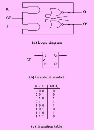
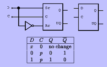
It is a change of the JK flip-flop. Timing Diagram of a Master Flip Flop. No change and Toggle.
The S and R inputs of the RS bistable have been replaced by. The flip flop will be disabled and Q remains unchanged when both the inputs of the JK flip flop set to 0. The Toggle_FlipFlop function block implements the truth table for T Toggle flip-flop with set priority.
First the D flip-flop is connected to an edge detector circuit which will detect the negative edge or positive edge of. The control logic or the control unit or the controller is used to. Description The Atmel750 architecture is twice as powerful as most other 24-pin programma- ble logic devices.
Flops sequential inputs flop problem. The circuit diagram of the JK Flip Flop is shown in the figure below. From the diagram it is evident that the flip flop has mainly four states.
Analyze the circuit given below find its truth table that. In electronics a flip-flop or latch is a circuit that has two stable states and can be used to store state information a bistable multivibratorThe circuit can be made to change state by signals. That means output of one D flip-flop is.
Flip-flop circuits are used for designing computer hardware such as CPU memory counter etc. Flip flop applications circuit. The IC power source V DD ranges from 0 to 7V and the data is available in the datasheet.
Use RS flip - flops. T Flip-flop Circuit diagram and Explanation. They are S1 R0Q1 Q0 This state is also called the SET state.
The four inputs are logic 1 logic 0. The Toggle_FlipFlop is a type of Flip-Flop which obeys this truth table. J-K 20 flip-flop is one of the most commonly used such type of flip-flop circuits.
11 State diagram of a 3-bit binary counter Solution. Marks 10 10 20 1. The Flip-Flop block has aluminum hardcoat-anodized side plates and features Hard Lube-anodized aluminum sheaves for strength and corrosion resistance.
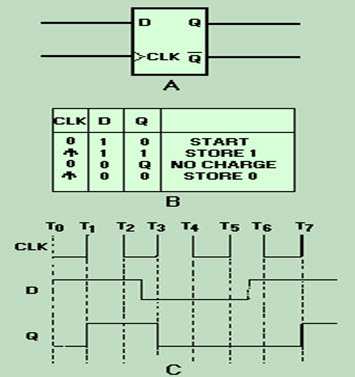
The circuit diagram of the edge triggered D type flip flop explained here. Block Diagram Features Advanced High-speed Electrically-erasable Programmable Logic Device Superset of 22V10 Enhanced Logic Flexibility Backward Compatible with. ECA ExpertsComputerAcademy SRFlipFlop SRLatchWhat is SR Flip Flop-----SR flip-flop is a gated set-reset flip-flop.
The term digital in electronics represents the data generation processing or storing in the form of two states.

Quasi Static Negative Edge Triggered D Flip Flop Circuit Layout A Download Scientific Diagram

Clocked T Flip Flop A Characteristic Table B Logic Circuits C Download Scientific Diagram
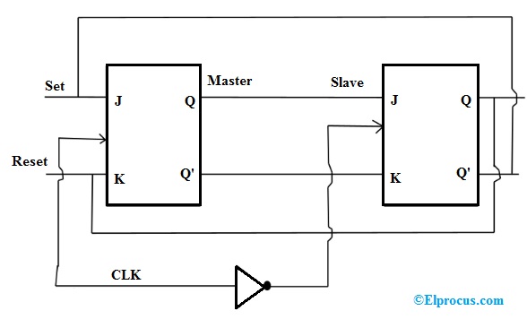
What Is A Master Slave Flip Flop Circuit Diagram And Its Working

A Conceptual Block Diagram Of A Non Volatile Flip Flop And B Download Scientific Diagram
Flip Flop Circuit Types And Its Applications
![]()
Schematic Diagram Of A Conventional D Flip Flop Download Scientific Diagram
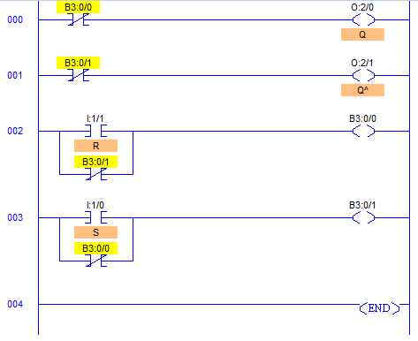
Plc Program To Implement Sr Flip Flop Sanfoundry
Flip Flop Circuit Types And Its Applications

Clocked T Flip Flop A Characteristic Table B Logic Circuits C Download Scientific Diagram
A Simple Bang Bang Loop Using A Flip Flop For A Phase Detector To Lock Download Scientific Diagram

Block Diagram Of The Flip Flop Circuit Download Scientific Diagram

Schematic Of Extravascular Administration With Flip Flop Kinetics Download Scientific Diagram

Logic Diagram Of J K Flip Flop Download Scientific Diagram
Test Circuit Schematic For Three Tag Flip Flops Each D Type Flip Flop Download Scientific Diagram

A Simple Bang Bang Loop Using A Flip Flop For A Phase Detector To Lock Download Scientific Diagram

A Conceptual Block Diagram Of A Non Volatile Flip Flop And B Download Scientific Diagram

Block Diagram Of The Flip Flop Circuit Download Scientific Diagram